


Journal of Vacuum Science & Technology
@jvstab.bsky.social
JVST A publishes research on interfaces & surfaces of materials, thin films, & plasmas.
JVST B covers microelectronics & nanotechnology, with a focus on processing, measurement, & phenomena associated with micrometer & nanometer structures & devices.
JVST B covers microelectronics & nanotechnology, with a focus on processing, measurement, & phenomena associated with micrometer & nanometer structures & devices.
Happy Holidays from our team! Wishing you the best during this holiday season and into the new year. We look forward to sharing more exciting research with you in 2026.✨

December 23, 2025 at 2:34 PM
Happy Holidays from our team! Wishing you the best during this holiday season and into the new year. We look forward to sharing more exciting research with you in 2026.✨
Featured on the latest #JVSTA cover, Joshua Wagner & Steven J. Sibener from the University of Chicago investigate how atomic oxygen affects the behavior of C₆₀ molecules on 2D materials.
Read the featured article here! doi.org/10.1116/6.00...
Read the featured article here! doi.org/10.1116/6.00...

December 22, 2025 at 5:36 PM
Featured on the latest #JVSTA cover, Joshua Wagner & Steven J. Sibener from the University of Chicago investigate how atomic oxygen affects the behavior of C₆₀ molecules on 2D materials.
Read the featured article here! doi.org/10.1116/6.00...
Read the featured article here! doi.org/10.1116/6.00...
Researchers from Tokyo Electron & TEL Technology Center, Americas demonstrate a novel etching process capable of fabricating 3D-NAND memory channel hole structures with a depth of 10 μm and an aspect ratio of 100.
doi.org/10.1116/6.00...
doi.org/10.1116/6.00...

Development for high-aspect-ratio hole etching with hydrogen fluoride gas based cryogenic process
We demonstrate a novel plasma process capable of etching the ONON (silicon oxide/silicon nitride) hole structure for manufacturing 3D-NAND devices with a depth
doi.org
December 19, 2025 at 3:04 PM
Researchers from Tokyo Electron & TEL Technology Center, Americas demonstrate a novel etching process capable of fabricating 3D-NAND memory channel hole structures with a depth of 10 μm and an aspect ratio of 100.
doi.org/10.1116/6.00...
doi.org/10.1116/6.00...
Electron beam generated plasmas are useful in the production of ion-ion plasmas due to their low electron temp. Authors examine characteristics of these plasmas in Ar/SF₆ & Ar/NF₃ mixtures, linking them to the efficacy of the F layer growth process.
doi.org/10.1116/6.00...
doi.org/10.1116/6.00...

Electron beam generated ion-ion plasmas produced in Ar/SF6 and Ar/NF3 mixtures for plasma anodization
In this work, electron beam generated plasmas in Ar/SF6 and Ar/NF3 mixtures are used to form ion-ion plasmas from which one can extract F− ions. These negative
doi.org
December 18, 2025 at 8:26 PM
Electron beam generated plasmas are useful in the production of ion-ion plasmas due to their low electron temp. Authors examine characteristics of these plasmas in Ar/SF₆ & Ar/NF₃ mixtures, linking them to the efficacy of the F layer growth process.
doi.org/10.1116/6.00...
doi.org/10.1116/6.00...
A major challenge in improving thermoelectric materials is understanding how structural & substrate effects impact performance. Here, authors study the effect various qualities of FeSi films grown on Si substrates have on key transport properties.
doi.org/10.1116/6.00...
doi.org/10.1116/6.00...

Crystal structure and thermoelectric efficiency of FeSi films on Si substrates: Shunting effects and first-principles calculations of lattice thermal conductivity
The crystal structure and thermoelectric parameters (conductivity, Seebeck coefficient, and power factor) of ultrathin (3–3.5 nm) stoichiometric monoclinic FeSi
doi.org
December 18, 2025 at 6:45 PM
A major challenge in improving thermoelectric materials is understanding how structural & substrate effects impact performance. Here, authors study the effect various qualities of FeSi films grown on Si substrates have on key transport properties.
doi.org/10.1116/6.00...
doi.org/10.1116/6.00...
Researchers from @caltech.edu are pushing electron-beam lithography to the true single-nanometer frontier! In this study, authors describe two new resists that can reliably pattern features as small as 5 nm—even in 100-nm-thick films.
doi.org/10.1116/6.00...
doi.org/10.1116/6.00...

Positive electron beam resists for lithography below 5 nm
We compare two promising new positive self-developing electron beam resists that enable the direct patterning of nanostructures at the 1–5 nm scale. Myo-inosito
doi.org
December 11, 2025 at 6:08 PM
Researchers from @caltech.edu are pushing electron-beam lithography to the true single-nanometer frontier! In this study, authors describe two new resists that can reliably pattern features as small as 5 nm—even in 100-nm-thick films.
doi.org/10.1116/6.00...
doi.org/10.1116/6.00...
A hybrid sputtering approach combining low-energy Cs+ with Ar-GCIB enhances inorganic sputtering while preserving organic signals, enabling accurate TOF-SIMS depth profiling of inorganic-organic multilayers.
doi.org/10.1116/6.00...
doi.org/10.1116/6.00...

Hybrid sputtering approach for reliable TOF-SIMS depth profiling of inorganic–organic multilayer films
Time-of-flight secondary ion mass spectrometry (TOF-SIMS) combined with argon gas cluster ion beam (Ar-GCIB) enables low-damage, high-resolution depth profiling
doi.org
December 10, 2025 at 5:32 PM
A hybrid sputtering approach combining low-energy Cs+ with Ar-GCIB enhances inorganic sputtering while preserving organic signals, enabling accurate TOF-SIMS depth profiling of inorganic-organic multilayers.
doi.org/10.1116/6.00...
doi.org/10.1116/6.00...
What hidden surface chemistry governs when ammonium fluorosilicate forms during SiNx etching—& why does it only sometimes cause an etch stop? Researchers from @coschoolofmines.bsky.social & @lamresearch.com explore variables impacting etching using ATR–FTIR spectroscopy. doi.org/10.1116/6.00...

Formation and stability of ammonium fluorosilicate during etching of SiNx in CH2F2/Ar and SF6/H2 plasmas
During reactive ion etching of SiNx in fluorine-based plasmas where HF is produced through a combination of gas-phase and surface reactions, ammonium fluorosili
doi.org
December 9, 2025 at 6:43 PM
What hidden surface chemistry governs when ammonium fluorosilicate forms during SiNx etching—& why does it only sometimes cause an etch stop? Researchers from @coschoolofmines.bsky.social & @lamresearch.com explore variables impacting etching using ATR–FTIR spectroscopy. doi.org/10.1116/6.00...
PtSi has lots of applications due to its unique metallic & superconducting properties, promising for the scalability of quantum computing systems.
Authors from @brookhavenlab.bsky.social Lab provide reference XPS data for the material for use as its applications expand.
doi.org/10.1116/6.00...
Authors from @brookhavenlab.bsky.social Lab provide reference XPS data for the material for use as its applications expand.
doi.org/10.1116/6.00...

Superconducting platinum silicide analyzed by x-ray photoelectron spectroscopy
Platinum silicide has garnered increased attention due to its potential applications as a superconductor within silicon technology. In this work, we characteriz
doi.org
December 8, 2025 at 8:29 PM
PtSi has lots of applications due to its unique metallic & superconducting properties, promising for the scalability of quantum computing systems.
Authors from @brookhavenlab.bsky.social Lab provide reference XPS data for the material for use as its applications expand.
doi.org/10.1116/6.00...
Authors from @brookhavenlab.bsky.social Lab provide reference XPS data for the material for use as its applications expand.
doi.org/10.1116/6.00...
Type-II band alignment in p-NiO/n-(AlGa)₂O₃ lets holes stay confined while electrons escape easily. Tunable offsets via Al content boost rectifier performance and guide next-gen power device design.
doi.org/10.1116/6.00...
doi.org/10.1116/6.00...

Al composition dependence of band alignment in NiO/(AlxGa1−x)2O3 heterojunctions
This study investigates the electronic band alignment of the p-NiO/n-(AlxGa1−x)2O3 heterojunction, a promising candidate for next-generation power electronics.
doi.org
December 8, 2025 at 8:09 PM
Type-II band alignment in p-NiO/n-(AlGa)₂O₃ lets holes stay confined while electrons escape easily. Tunable offsets via Al content boost rectifier performance and guide next-gen power device design.
doi.org/10.1116/6.00...
doi.org/10.1116/6.00...
Cryogenic ToF-SIMS imaging preserved native lipid distributions in 3D spheroids, unlike air-dried samples that caused water loss and lipid migration artifacts. doi.org/10.1116/6.00...

Cryogenic ToF-SIMS 3D imaging of SKOV3 ovarian cancer spheroids: Preserving native lipid distributions with Ar cluster sputtering
Mass spectrometry imaging (MSI) enables spatial mapping of molecular distributions in biological samples, but the reliability of results strongly depends on sam
doi.org
December 5, 2025 at 2:52 PM
Cryogenic ToF-SIMS imaging preserved native lipid distributions in 3D spheroids, unlike air-dried samples that caused water loss and lipid migration artifacts. doi.org/10.1116/6.00...
Authors from the U.S. Naval Research Laboratory & Purdue University utilize #ALDep of Al₂O₃ on BNNT fabrics to enhance their high-temperature stability limit, a method that could potentially to do the same for other nanoporous materials.
doi.org/10.1116/6.00...
doi.org/10.1116/6.00...
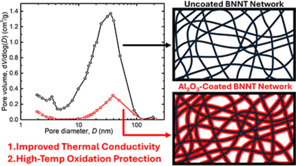
Dual-purpose alumina ALD coatings for enhanced oxidation resistance and thermal conductivity of boron nitride nanotube fabrics
Boron nitride remains a critical material for myriad applications requiring high-temperature stability and thermal management. This work explores the utilizatio
doi.org
December 4, 2025 at 9:03 PM
Authors from the U.S. Naval Research Laboratory & Purdue University utilize #ALDep of Al₂O₃ on BNNT fabrics to enhance their high-temperature stability limit, a method that could potentially to do the same for other nanoporous materials.
doi.org/10.1116/6.00...
doi.org/10.1116/6.00...
Low-temp #ALDep supercycles insert trace Al into TiN, forming TiAlN with a tunable effective work function while keeping conductivity—enabling a dual-compatible metal-gate electrode for both n-type & p-type MOSFETs.
doi.org/10.1116/6.00...
doi.org/10.1116/6.00...

Work function tuning in TiAlN thin films by trace Al doping for CMOS-compatible metal gates
With continued scaling of semiconductor devices, integrating high-k dielectrics with metal-gate electrodes is essential to overcome the limitations of conventio
doi.org
December 3, 2025 at 7:12 PM
Low-temp #ALDep supercycles insert trace Al into TiN, forming TiAlN with a tunable effective work function while keeping conductivity—enabling a dual-compatible metal-gate electrode for both n-type & p-type MOSFETs.
doi.org/10.1116/6.00...
doi.org/10.1116/6.00...
Authors from @helsinki.fi describe a self-limiting #ALEtch process for etching molybdenum using O₂ + NbCl₅ - offering isotropic & selective etching with high control. Promising for the future development of interconnects for microelectronics!
doi.org/10.1116/6.00...
doi.org/10.1116/6.00...

Atomic layer etching of molybdenum with O2 and NbCl5
Molybdenum is a material of significant interest in the development of future interconnects for microelectronics. This is due to a slower increase in resistivit
doi.org
November 25, 2025 at 7:39 PM
Authors from @helsinki.fi describe a self-limiting #ALEtch process for etching molybdenum using O₂ + NbCl₅ - offering isotropic & selective etching with high control. Promising for the future development of interconnects for microelectronics!
doi.org/10.1116/6.00...
doi.org/10.1116/6.00...
Direct atomic layer processing breaks #ALDep free from vacuum limits!
It prints ALD-quality TiO₂ layers at ambient pressure with no overspray, ultra-smooth films, & at speeds up to 200 mm/s—high-throughput, precision nanofab made easy.
doi.org/10.1116/6.00...
It prints ALD-quality TiO₂ layers at ambient pressure with no overspray, ultra-smooth films, & at speeds up to 200 mm/s—high-throughput, precision nanofab made easy.
doi.org/10.1116/6.00...
doi.org
November 24, 2025 at 8:10 PM
Direct atomic layer processing breaks #ALDep free from vacuum limits!
It prints ALD-quality TiO₂ layers at ambient pressure with no overspray, ultra-smooth films, & at speeds up to 200 mm/s—high-throughput, precision nanofab made easy.
doi.org/10.1116/6.00...
It prints ALD-quality TiO₂ layers at ambient pressure with no overspray, ultra-smooth films, & at speeds up to 200 mm/s—high-throughput, precision nanofab made easy.
doi.org/10.1116/6.00...
New #machinelearning modeling approach called ST-GWP combines self-training and ensemble methods to predict global warming potential with high accuracy & no experiments. # of halogen atoms and electron properties are key factors. doi.org/10.1116/6.00...

Predicting global warming potential: A self-training and ensemble machine learning approach
Amid growing concerns about global warming, a critical challenge for the semiconductor industry is the development of materials with low global warming potentia
doi.org
November 21, 2025 at 8:48 PM
New #machinelearning modeling approach called ST-GWP combines self-training and ensemble methods to predict global warming potential with high accuracy & no experiments. # of halogen atoms and electron properties are key factors. doi.org/10.1116/6.00...
Tabletop EUV system enables quick, reliable testing of photoresists, supporting faster R&D for next-gen semiconductor manufacturing. doi.org/10.1116/6.00...

Photoresist characterization using a tabletop extreme ultraviolet source at 30 nm wavelength
In this paper, we investigate the viability of using ZEP520A, a commercially available electron-beam photoresist, as a positive resist for extreme ultraviolet (
doi.org
November 21, 2025 at 2:52 PM
Tabletop EUV system enables quick, reliable testing of photoresists, supporting faster R&D for next-gen semiconductor manufacturing. doi.org/10.1116/6.00...
Graphene solar cells power IoT sensors with no batteries! ☀️
Authors from @uarkansas.bsky.social & @umich.edu show how series-connected cells charge capacitors in minutes, running a temperature sensor for 24+ hours—ultralow power, long-life, fully autonomous.
doi.org/10.1116/6.00...
Authors from @uarkansas.bsky.social & @umich.edu show how series-connected cells charge capacitors in minutes, running a temperature sensor for 24+ hours—ultralow power, long-life, fully autonomous.
doi.org/10.1116/6.00...

Array of mini-graphene-silicon solar cells intermittently recharges storage capacitors powering a temperature sensor
Developing autonomous sensor systems that draw power from the ambient environment is a critical step for creating the Internet of Things. In this study, the aut
doi.org
November 19, 2025 at 3:45 PM
Graphene solar cells power IoT sensors with no batteries! ☀️
Authors from @uarkansas.bsky.social & @umich.edu show how series-connected cells charge capacitors in minutes, running a temperature sensor for 24+ hours—ultralow power, long-life, fully autonomous.
doi.org/10.1116/6.00...
Authors from @uarkansas.bsky.social & @umich.edu show how series-connected cells charge capacitors in minutes, running a temperature sensor for 24+ hours—ultralow power, long-life, fully autonomous.
doi.org/10.1116/6.00...
A new suspended Ge-on-Si infrared absorber design with backside holes + an Al reflector boosts 1550-nm absorbance to 59% and doubles responsivity. Big promise for the future of optoelectronics!
doi.org/10.1116/6.00...
doi.org/10.1116/6.00...

Broadband optical enhancement of suspended Ge-on-Si infrared absorbers by using backside etching holes and a metallic reflector
This work introduces a method for developing a suspended Ge-on-Si structure aimed at improving infrared absorption for photodetector applications. Traditional G
doi.org
November 18, 2025 at 8:18 PM
A new suspended Ge-on-Si infrared absorber design with backside holes + an Al reflector boosts 1550-nm absorbance to 59% and doubles responsivity. Big promise for the future of optoelectronics!
doi.org/10.1116/6.00...
doi.org/10.1116/6.00...
Researchers from USC create an analog stochastic Boolean satisfiability solver and accelerate multiple patterning layout decomposition by 100× through inherent parallelism, enabling faster NP-complete problem solving in VLSI design. doi.org/10.1116/6.00...
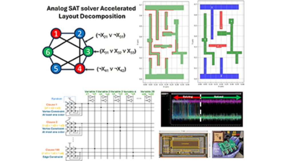
Accelerating multiple patterning lithography layout decomposition with a stochastic analog Boolean satisfiability solver
This work presents a stochastic analog SAT solver to address the computational bottleneck in multiple patterning lithography layout decomposition. The decomposi
doi.org
November 17, 2025 at 7:44 PM
Researchers from USC create an analog stochastic Boolean satisfiability solver and accelerate multiple patterning layout decomposition by 100× through inherent parallelism, enabling faster NP-complete problem solving in VLSI design. doi.org/10.1116/6.00...
Reposted by Journal of Vacuum Science & Technology

📢Attention #ALDep and #ALEtch researchers - #ALDALE2026 is now accepting abstracts through February 5. Join us in 🌴Tampa, FL for the AVS 26th International Conference on Atomic Layer Deposition & the 13th Atomic Layer Etching Workshop. #AtomicLayerDeposition #AtomicLayerEtching ald2026.avs.org

November 17, 2025 at 7:19 PM
📢Attention #ALDep and #ALEtch researchers - #ALDALE2026 is now accepting abstracts through February 5. Join us in 🌴Tampa, FL for the AVS 26th International Conference on Atomic Layer Deposition & the 13th Atomic Layer Etching Workshop. #AtomicLayerDeposition #AtomicLayerEtching ald2026.avs.org
Featured on our most recent #JVSTB cover, researchers from AIST in Japan highlight the critical importance of interparticle contact in optimizing all-solid-state battery performance, offering valuable insights for improving battery design.🔋
doi.org/10.1116/6.00...
doi.org/10.1116/6.00...

November 12, 2025 at 6:33 PM
Featured on our most recent #JVSTB cover, researchers from AIST in Japan highlight the critical importance of interparticle contact in optimizing all-solid-state battery performance, offering valuable insights for improving battery design.🔋
doi.org/10.1116/6.00...
doi.org/10.1116/6.00...
Researchers from @thermofishersci.bsky.social investigate emission profiles & uniformity of electron emitters with varying radii, enabling end-users to choose the best emitters for their needs, including enhancing multibeam applications.
doi.org/10.1116/6.00...
doi.org/10.1116/6.00...

Angular emission evolution of the ZrO/W(100) Schottky emitter
An investigation of the uniformity and evolution of the angular emission distribution of the ZrO/W(100) Schottky emitter operated at an angular intensity of 1.0
doi.org
November 11, 2025 at 8:46 PM
Researchers from @thermofishersci.bsky.social investigate emission profiles & uniformity of electron emitters with varying radii, enabling end-users to choose the best emitters for their needs, including enhancing multibeam applications.
doi.org/10.1116/6.00...
doi.org/10.1116/6.00...
Compared to commercial Si x-ray detectors, a Ni/Au β-Ga₂O₃ Schottky barrier diode shows 14× higher sensitivity at 500 K with fast response & low noise — ideal for harsh environments. doi.org/10.1116/6.00...

Effect of space charge-limited mechanism on the x-ray detection performance of Ni/Au β-Ga2O3 Schottky diode at high temperature
Gallium oxide-based (Ga2O3) detectors have shown great potential for x-ray detection. In specific high-temperature environmental application scenarios such as p
doi.org
November 10, 2025 at 7:32 PM
Compared to commercial Si x-ray detectors, a Ni/Au β-Ga₂O₃ Schottky barrier diode shows 14× higher sensitivity at 500 K with fast response & low noise — ideal for harsh environments. doi.org/10.1116/6.00...
New study from @helsinki.fi shows phenol can selectively block Ru growth in AS-ALD. Phenol inhibits Ru on W, TiN, HfO₂ & ZrO₂, enabling high selectivity (>0.8) for up to 1000 ALD cycles.
doi.org/10.1116/6.00...
doi.org/10.1116/6.00...

Area selective atomic layer deposition of ruthenium with phenol as a small molecule inhibitor
A study on area selective atomic layer deposition (AS-ALD) of ruthenium was performed using phenol as a small molecule inhibitor (SMI). The surfaces studied wer
doi.org
October 30, 2025 at 5:12 PM
New study from @helsinki.fi shows phenol can selectively block Ru growth in AS-ALD. Phenol inhibits Ru on W, TiN, HfO₂ & ZrO₂, enabling high selectivity (>0.8) for up to 1000 ALD cycles.
doi.org/10.1116/6.00...
doi.org/10.1116/6.00...