


Marco A. Lopez-Sanchez
@marcoalopez.fediscience.org.ap.brid.gy
An Earth scientist interested in rock/mineral properties working at the Andalusian Earth Sciences Institute (IACT-CSIC) in Granada (Spain). I like to code […]
[bridged from https://fediscience.org/@marcoalopez on the fediverse by https://fed.brid.gy/ ]
[bridged from https://fediscience.org/@marcoalopez on the fediverse by https://fed.brid.gy/ ]
Reposted by Marco A. Lopez-Sanchez
Ho, ho, ho: un grupo autodenominado Robin de los Callejones entra en un supermercado de Montreal disfrazado de Papá Noel y sus elfos, hace una compra por valor de 1.900 euros y se va sin pagar —repartiendo el botín bajo un árbol de Navidad y donando el resto a bancos de alimentos […]
Original post on journa.host
journa.host
December 18, 2025 at 8:38 PM
Ho, ho, ho: un grupo autodenominado Robin de los Callejones entra en un supermercado de Montreal disfrazado de Papá Noel y sus elfos, hace una compra por valor de 1.900 euros y se va sin pagar —repartiendo el botín bajo un árbol de Navidad y donando el resto a bancos de alimentos […]
Nice visualisation of the sources of electricity generation in Spain over time. https://public.flourish.studio/visualisation/26800152/
December 14, 2025 at 4:42 PM
Nice visualisation of the sources of electricity generation in Spain over time. https://public.flourish.studio/visualisation/26800152/
Reposted by Marco A. Lopez-Sanchez

Today we are calling on institutions around the world to take control of their #digitalsovereignty, including their social accounts. Governments should communicate directly with their citizens on open platforms, not through the mouthpiece of a corporation […]
Original post on mastodon.social
mastodon.social
December 9, 2025 at 11:07 AM
Today we are calling on institutions around the world to take control of their #digitalsovereignty, including their social accounts. Governments should communicate directly with their citizens on open platforms, not through the mouthpiece of a corporation […]
I think this is a very interesting and fresh take on AI and LLMs. It's long but worth reading: The Reverse Centaur’s Guide to Criticizing AI https://pluralistic.net/2025/12/05/pop-that-bubble/#u-washington
December 8, 2025 at 9:31 PM
I think this is a very interesting and fresh take on AI and LLMs. It's long but worth reading: The Reverse Centaur’s Guide to Criticizing AI https://pluralistic.net/2025/12/05/pop-that-bubble/#u-washington
Reposted by Marco A. Lopez-Sanchez

Linux Tech Tips: _There was a recent thing from a major tech company where developers were asked to say how many lines of code they wrote, and if it wasn’t enough, they were terminated. And there was someone here who was extremely upset about that approach to measuring productivity because it […]
Original post on manganiello.eu
manganiello.eu
December 6, 2025 at 9:26 AM
Linux Tech Tips: _There was a recent thing from a major tech company where developers were asked to say how many lines of code they wrote, and if it wasn’t enough, they were terminated. And there was someone here who was extremely upset about that approach to measuring productivity because it […]
Reposted by Marco A. Lopez-Sanchez
Agricultura señala que el brote de peste porcina salió del laboratorio de Bellaterra
https://www.lavanguardia.com/natural/20251206/11337027/agricultura-senala-brote-peste-porcina-salio-laboratorio-bellaterra.html
> La cepa que mata jabalíes, Georgia 2007, no circula en el medio natural, pero […]
https://www.lavanguardia.com/natural/20251206/11337027/agricultura-senala-brote-peste-porcina-salio-laboratorio-bellaterra.html
> La cepa que mata jabalíes, Georgia 2007, no circula en el medio natural, pero […]
Original post on mstdn.science
mstdn.science
December 6, 2025 at 8:58 AM
Agricultura señala que el brote de peste porcina salió del laboratorio de Bellaterra
https://www.lavanguardia.com/natural/20251206/11337027/agricultura-senala-brote-peste-porcina-salio-laboratorio-bellaterra.html
> La cepa que mata jabalíes, Georgia 2007, no circula en el medio natural, pero […]
https://www.lavanguardia.com/natural/20251206/11337027/agricultura-senala-brote-peste-porcina-salio-laboratorio-bellaterra.html
> La cepa que mata jabalíes, Georgia 2007, no circula en el medio natural, pero […]
Reposted by Marco A. Lopez-Sanchez
Quite a big #earthquake in South Spain one hour ago, but also relatively deep and therefore not as intense even at the epicenter. ⚒️🧪 #terremoto

December 5, 2025 at 10:54 AM
Quite a big #earthquake in South Spain one hour ago, but also relatively deep and therefore not as intense even at the epicenter. ⚒️🧪 #terremoto
Reposted by Marco A. Lopez-Sanchez

Se han localizado dos jabalíes muertos por un brote de peste porcina africana (PPA) en la provincia de Barcelona. Se trata de una enfermedad vírica —un asfivirus— que afecta a súidos —jabalíes, cerdos domésticos, facóqueros y otras especies afines— y que presenta una tasa de morbilidad […]
Original post on neopaquita.es
neopaquita.es
November 28, 2025 at 11:39 AM
Se han localizado dos jabalíes muertos por un brote de peste porcina africana (PPA) en la provincia de Barcelona. Se trata de una enfermedad vírica —un asfivirus— que afecta a súidos —jabalíes, cerdos domésticos, facóqueros y otras especies afines— y que presenta una tasa de morbilidad […]
Reposted by Marco A. Lopez-Sanchez

@euklidiadas @agaitaarino lo siento pero eso no está bien. La media de toneladas de emisiones por persona y año está por debajo de las 5 toneladas a nivel mundial, y por debajo de las 15 para el país que más emite per cápita (EE.UU.)¹ así que decir que tener un hijo menos ahorra 60 toneladas/año […]
Original post on neopaquita.es
neopaquita.es
November 29, 2025 at 10:08 AM
@euklidiadas @agaitaarino lo siento pero eso no está bien. La media de toneladas de emisiones por persona y año está por debajo de las 5 toneladas a nivel mundial, y por debajo de las 15 para el país que más emite per cápita (EE.UU.)¹ así que decir que tener un hijo menos ahorra 60 toneladas/año […]
Reposted by Marco A. Lopez-Sanchez

FLUJO INTENSO DEL NORTE = ONDAS DE MONTAÑA
🏔️〰️
🏔️〰️

November 21, 2025 at 10:31 AM
FLUJO INTENSO DEL NORTE = ONDAS DE MONTAÑA
🏔️〰️
🏔️〰️
Reposted by Marco A. Lopez-Sanchez

Ahí va mi clásico de todos los otoños con los datos de los notarios para desmontar la propaganda sobre el impuesto de sucesiones, la misma tasa de renuncias a herencias en Asturias que en Andalucía aunque aumentaran la exención al millón de euros
www.lavozdeasturias.es/noticia/astu...
www.lavozdeasturias.es/noticia/astu...

Asturias registra tantas renuncias a herencias como las comunidades que subieron la exención al millón de euros
Los datos de los notarios revelan que los desestimientos en el Principado son iguales que en La Rioja y Andalucía
www.lavozdeasturias.es
November 15, 2025 at 8:03 AM
Ahí va mi clásico de todos los otoños con los datos de los notarios para desmontar la propaganda sobre el impuesto de sucesiones, la misma tasa de renuncias a herencias en Asturias que en Andalucía aunque aumentaran la exención al millón de euros
www.lavozdeasturias.es/noticia/astu...
www.lavozdeasturias.es/noticia/astu...
Reposted by Marco A. Lopez-Sanchez

#bcnspiracy25 #updatespiracy Clara Grima nos relata lo complicado que era la búsqueda de Ceres, que al final culminó Gauss. Desarrolló el algoritmo de mínimos cuadrados para determinar la elipse de la órbita de Ceres a partir de los datos astronómicos disponibles.


November 15, 2025 at 11:48 AM
#bcnspiracy25 #updatespiracy Clara Grima nos relata lo complicado que era la búsqueda de Ceres, que al final culminó Gauss. Desarrolló el algoritmo de mínimos cuadrados para determinar la elipse de la órbita de Ceres a partir de los datos astronómicos disponibles.
Reposted by Marco A. Lopez-Sanchez

Okay, but hear me out, what if we produce an entire generation of students who are *all* the ones who did nothing in the group project?
November 13, 2025 at 5:03 AM
Okay, but hear me out, what if we produce an entire generation of students who are *all* the ones who did nothing in the group project?
Reposted by Marco A. Lopez-Sanchez

This is #copper. The exquisite golden tetrahexahedral crystal glows with its own light. And the amazing bevels (look closely) and faces! Only nature could create something so beautiful. Vote for Copper Ore. It has it all. Link in ALT.
#OreCup ⚒️ sci-fi 🧪 🖖🏼 scifi Geosciences #WomenInSTEM geology 🍎 🔭🪐
#OreCup ⚒️ sci-fi 🧪 🖖🏼 scifi Geosciences #WomenInSTEM geology 🍎 🔭🪐

November 9, 2025 at 10:09 PM
This is #copper. The exquisite golden tetrahexahedral crystal glows with its own light. And the amazing bevels (look closely) and faces! Only nature could create something so beautiful. Vote for Copper Ore. It has it all. Link in ALT.
#OreCup ⚒️ sci-fi 🧪 🖖🏼 scifi Geosciences #WomenInSTEM geology 🍎 🔭🪐
#OreCup ⚒️ sci-fi 🧪 🖖🏼 scifi Geosciences #WomenInSTEM geology 🍎 🔭🪐
Reposted by Marco A. Lopez-Sanchez

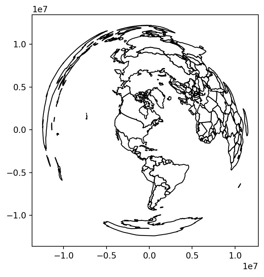
Confused about coordinate reference systems (CRSs)? 🧭🌍🐍
Chapter 6 of Geocomputation with Python dives into:
- Geographic vs projected CRSs (lon/lat vs meters)
- Getting, setting & reprojecting CRSs
- Why ignoring CRSs can break your analysis 🚨
👉 […]
[Original post on fosstodon.org]
Chapter 6 of Geocomputation with Python dives into:
- Geographic vs projected CRSs (lon/lat vs meters)
- Getting, setting & reprojecting CRSs
- Why ignoring CRSs can break your analysis 🚨
👉 […]
[Original post on fosstodon.org]
November 9, 2025 at 2:02 PM
Confused about coordinate reference systems (CRSs)? 🧭🌍🐍
Chapter 6 of Geocomputation with Python dives into:
- Geographic vs projected CRSs (lon/lat vs meters)
- Getting, setting & reprojecting CRSs
- Why ignoring CRSs can break your analysis 🚨
👉 […]
[Original post on fosstodon.org]
Chapter 6 of Geocomputation with Python dives into:
- Geographic vs projected CRSs (lon/lat vs meters)
- Getting, setting & reprojecting CRSs
- Why ignoring CRSs can break your analysis 🚨
👉 […]
[Original post on fosstodon.org]
source: XKCD at https://xkcd.com/3165/

November 8, 2025 at 6:41 PM
source: XKCD at https://xkcd.com/3165/
Reposted by Marco A. Lopez-Sanchez


Reposted by Marco A. Lopez-Sanchez
Reposted by Marco A. Lopez-Sanchez

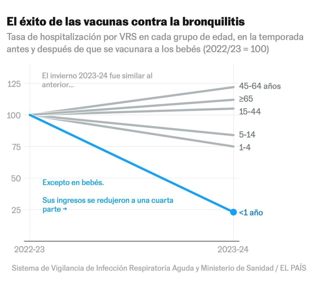
En 2023, Españita comenzó a ponerle a todes les bebés la vacuna del virus respiratorio sincitial. Resultado: 10.000 hospitalizaciones menos por bronquiolitis. Viva la ciencia.
October 26, 2025 at 2:05 PM
En 2023, Españita comenzó a ponerle a todes les bebés la vacuna del virus respiratorio sincitial. Resultado: 10.000 hospitalizaciones menos por bronquiolitis. Viva la ciencia.
Reposted by Marco A. Lopez-Sanchez

Oof.
Those "AI Browsers" are a real privacy hell
Personally, I strongly recommend NOT to use these
Those "AI Browsers" are a real privacy hell
Personally, I strongly recommend NOT to use these
October 24, 2025 at 9:34 PM
Oof.
Those "AI Browsers" are a real privacy hell
Personally, I strongly recommend NOT to use these
Those "AI Browsers" are a real privacy hell
Personally, I strongly recommend NOT to use these
JupyterGIS breaks through to the next level https://eo4society.esa.int/2025/10/16/jupytergis-breaks-through-to-the-next-level/

JupyterGIS breaks through to the next level
Launched in June 2024, JupyterGIS was introduced as a collaborative, web-based GIS environment built on the JupyterLab framework. Its objective is to bring QGIS-inspired workflows into the browser, enabling real-time collaborative editing, seamless integration with notebooks, and support for core geospatial data formats.
When it was first announced earlier this year, JupyterGIS already delivered:
* Real-time collaborative editing (Google Docs-style)
* Visualisation of raster & vector data
* Symbology editing and spatio-temporal animations
* Programmatic map control via a Python API.
Thanks to contributions from the community and support from partner organizations, JupyterGIS has advanced significantly and now offers an expanded range of features for analysis, visualization, and collaboration.
**Enhanced vector tile capabilities**
Support for vector tiles has been strengthened, including full compatibility with the _pmtiles_ format.
Other key updates include:
* An _identify tool_ that inspects vector tiles to display features and associated properties.
* A _symbology panel_ that applies graduated, categorized, and canonical symbology to vector tile layers.
These improvements enhance the interpretability and styling of geospatial datasets directly in the browser.
The identify tool in action with a pmtiles vector dataset.
The symbology panel in action, allowing for different notations.
**A new processing toolbox**
One of the most significant updates is a new browser-based processing toolbox powered by a WebAssembly (WASM) build of the Geospatial Data Abstraction Library (GDAL).
Available tools include:
* _Buffer_ : computes a buffer around geometries of a vector dataset.
* _Convex Hull_ : calculates the convex hull for each feature of an input layer.
* _Dissolve_ : combines features of vector layers into new features
* _Bounding Boxes_ : calculates the bounding box for each feature in an input layer.
* _Centroid_ : creates a new layer with the centroids of the geometries of an input layer.
* _Concave Hull_ : computes the concave hull for each feature of an input point layer.
This toolbox has been designed for extensibility, with a JSON schema that allows additional GDAL operations to be integrated in a straightforward manner.
Using the processing tool to compute the convex hulls of geometries.
**Symbology enhancements**
Visualization of geospatial data has become more flexible and expressive through several enhancements:
* _Viridis_ is now the default colormap, providing perceptually uniform visualization.
* _Multiband symbology_ is now available for GeoTIFFs.
* _Canonical symbology_ defined in GeoJSON files can be applied automatically.
* _Colormaps_ can now be _reversed_ , allowing greater flexibility for data interpretation and visualization.
* In the case of _point layers_ , color and marker size can be styled independently, and bound to different data.
Setting color and radius based on data.
**Integration with SpatioTemporal Asset Catalogs (STAC)**
A SpatioTemporal Asset Catalog (STAC) browser is now embedded into JupyterGIS, streamlining access to different data collections. Users can select specific platforms and sensors, choose data products and processing levels, and set temporal and spatial constraints.
It is now possible to search across multiple datasets simultaneously. Users can click on any result to add it directly as a layer to their JupyterGIS project. This creates a seamless workflow from data discovery to visualization, making it easier for researchers and analysts to find and integrate relevant satellite imagery and geospatial datasets into their Jupyter notebooks.
Currently, the STAC Browser only supports the Geodes STAC API but support for all STAC catalogs is under way.
Browsing a STAC access catalog from JupyterGIS.
**Support for more data types**
The range of supported geospatial data formats is now broadened with _GeoParquet_ and _PMTiles_**,** enabling efficient columnar storage and fast analytical queries for GeoParquet, and highly compact, streaming-friendly vector tile delivery for PMTiles.
**User experience and interface improvements**
The interface has been refined for a smoother workflow:
* _Integrated control panels_ (layer list, filters, layer properties, etc.), reducing back and forth between the JupyterLab side-panels and the JupyterGIS UI. It also improves the “single document” scenario, allowing it to interact with JupyterGIS controls when opening a GIS document from the classic Jupyter Notebook UI.
* An improved _toolbar design_ , with cleaner icons and better usability.
* A new feature to center the map on your _current location_.
* _Map annotations_ now link to the map: clicking an annotation automatically re-centers and zooms to the location.
* _Full-screen_ mode support.
**Legends for vector layers**
JupyterGIS now automatically generates legends for vector layers, ensuring consistent interpretation:
* Legends are dynamically updated to reflect current symbology.
* Customizations such as reversed colormaps are preserved.
Displaying legends in the layers panel.
**JupyterGIS tiler extension**
An extension for JupyterGIS enables the creation of JupyterGIS layers from _xarray variables_ in Jupyter kernels, with support for lazy evaluation, bridging geospatial workflows with powerful array-based computation.
The package, called JupyterGIS-tiler, is available in GitHub here and can be installed from PyPI with _pip install jupytergis-tiler_.
**Looking ahead**
Development will continue to expand JupyterGIS in several directions:
* Extension of the GDAL-based processing toolbox.
* Deeper integration with QGIS and a richer Python API for automation.
* A Story Maps Editor and Viewer to enable interactive communication of geospatial information through text, imagery, and maps.
In the meantime, feel free to try JupyterGIS directly in your browser with JupyterLite, no installation required.
Opportunities for engagement also include:
* Checking out documentation for tutorials and the Python API.
* Discussions via the GeoJupyter Zulip channel or the bi-weekly GeoJupyter hackathon.
* Contributions to the development repository.
The JupyterGIS community continues to grow, and active participation from researchers, developers, and educators worldwide is encouraged.
eo4society.esa.int
October 24, 2025 at 6:02 AM
JupyterGIS breaks through to the next level https://eo4society.esa.int/2025/10/16/jupytergis-breaks-through-to-the-next-level/
Diamond Thermal Conductivity: A New Era in Chip Cooling https://spectrum.ieee.org/diamond-thermal-conductivity

Diamond Blankets Will Keep Future Chips Cool
**Today’s****stunning computing power** is allowing us to move from human intelligence toward artificial intelligence. And as our machines gain more power, they’re becoming not just tools but decision-makers shaping our future.
But with great power comes great…heat!
As nanometer-scale transistors switch at gigahertz speeds, electrons race through circuits, losing energy as heat—which you feel when your laptop or your phone toasts your fingers. As we’ve crammed more and more transistors onto chips, we’ve lost the room to release that heat efficiently. Instead of the heat spreading out quickly across the silicon, which makes it much easier to remove, it builds up to form hot spots, which can be tens of degrees warmer than the rest of the chip. That extreme heat forces systems to throttle the performance of CPUs and GPUs to avoid degrading the chips.
In other words, what began as a quest for miniaturization has turned into a battle against thermal energy. This challenge extends across all electronics. In computing, high-performance processors demand ever-increasing power densities. (New Nvidia GPU B300 servers will consume nearly 15 kilowatts of power.) In communication, both digital and analog systems push transistors to deliver more power for stronger signals and faster data rates. In the power electronics used for energy conversion and distribution, efficiency gains are being countered by thermal constraints.
The ability to grow large-grained polycrystalline diamond at low temperature led to a new way to combat heat in transistors. Mohamadali Malakoutian
Rather than allowing heat to build up, what if we could spread it out right from the start, inside the chip?—diluting it like a cup of boiling water dropped into a swimming pool. Spreading out the heat would lower the temperature of the most critical devices and circuits and let the other time-tested cooling technologies work more efficiently. To do that, we’d have to introduce a highly thermally conductive material inside the IC, mere nanometers from the transistors, without messing up any of their very precise and sensitive properties. Enter an unexpected material—diamond.
###
In some ways, diamond is ideal. It’s one of the most thermally conductive materials on the planet—many times more efficient than copper—yet it’s also electrically insulating. However, integrating it into chips is tricky: Until recently we knew how to grow it only at circuit-slagging temperatures in excess of 1,000 °C.
But my research group at Stanford University has managed what seemed impossible. We can now grow a form of diamond suitable for spreading heat, directly atop semiconductor devices at low enough temperatures that even the most delicate interconnects inside advanced chips will survive. To be clear, this isn’t the kind of diamond you see in jewelry, which is a large single crystal. Our diamonds are a polycrystalline coating no more than a couple of micrometers thick.
The potential benefits could be huge. In some of our earliest gallium-nitride radio-frequency transistors, the addition of diamond dropped the device temperature by more than 50 °C. At the lower temperature, the transistors amplified X-band radio signals five times as well as before. We think our diamond will be even more important for advanced CMOS chips. Researchers predict that upcoming chipmaking technologies could make hot spots almost 10 °C hotter [see , “Future Chips Will Be Hotter Than Ever”, in this issue]. That’s probably why our research is drawing intense interest from the chip industry, including Applied Materials, Samsung, and TSMC. If our work continues to succeed as it has, heat will become a far less onerous constraint in CMOS and other electronics too.
## Where Heat Begins and Ends in Chips
At the boundary between the diamond and the semiconductor, a thin layer of silicon carbide forms. It acts as a bridge for heat to flow into the diamond. Mohamadali Malakoutian
Heat starts within transistors and the interconnects that link them, as the flow of current meets resistance. That means most of it is generated near the surface of the semiconductor substrate. From there it rises either through layers of metal and insulation or through the semiconductor itself, depending on the package architecture. The heat then encounters a thermal interface material designed to spread it out before it ultimately reaches a heat sink, a radiator, or some sort of liquid cooling, where air or fluid carries the heat away.
The dominant cooling strategies today center around advances in heat sinks, fans, and radiators. In pursuit of even better cooling, researchers have explored liquid cooling using microfluidic channels and removing heat using phase-change materials. Some computer clusters go so far as to submerge the servers in thermally conductive, dielectric—electrically insulating—liquids.
These innovations are critical steps forward, but they still have limitations. Some are so expensive they’re worthwhile only for the highest-performing chips; others are simply too bulky for the job. (Your smartphone can’t carry a conventional fan.) And none are likely to be very effective as we move toward chip architectures resembling silicon skyscrapers that stack multiple layers of chips. Such 3D systems are only as viable as our ability to remove heat from every layer within it.
The big problem is that chip materials are poor heat conductors, so the heat becomes trapped and concentrated, causing the temperature to skyrocket within the chip. At higher temperatures, transistors leak more current, wasting power; they age more quickly, too.
Heat spreaders allow the heat to move laterally, diluting it and allowing the circuits to cool. But they’re positioned far—relatively, of course—from where the heat is generated, and so they’re of little help with these hot spots. We need a heat-spreading technology that can exist within nanometers of where the heat is generated. This is where our new low-temperature diamond could be essential.
## How to Make Diamonds
Before my lab turned to developing diamond as a heat-spreading material, we were working on it as a semiconductor. In its single-crystal form—like the kind on your finger—it has a wide bandgap and ability to withstand enormous electric fields. Single-crystalline diamond also offers some of the highest thermal conductivity recorded in any material, reaching 2,200 to 2,400 watts per meter per kelvin—roughly six times as conductive as copper. Polycrystalline diamond—an easier to make material—can approach these values when grown thick. Even in this form, it outperforms copper.
As attractive as diamond transistors might be, I was keenly aware—based on my experience researching gallium nitride devices—of the long road ahead. The problem is one of scale. Several companies are working to scale high-purity diamond substrates to 50, 75, and even 100 millimeters but the diamond substrates we could acquire commercially were only about 3 mm across.
Gallium nitride high-electron-mobility transistors were an ideal test case for diamond cooling. The devices are 3D and the critical heat-generating part, the two-dimensional electron gas, is close to the surface. Chris Philpot
So we decided instead to try growing diamond films on large silicon wafers, in the hope of moving toward commercial-scale diamond substrates. In general, this is done by reacting methane and hydrogen at high temperatures, 900 °C or more. This results in not a single crystal but a forest of narrow columns. As they grow taller, the nanocolumns coalesce into a uniform film, but by the time they form high-quality polycrystalline diamond, the film is already very thick. This thick growth adds stress to the material and often leads to cracking and other problems.
But what if we used this polycrystalline coating as a heat spreader for other devices? If we could get diamond to grow within nanometers of transistors, get it to spread heat both vertically and laterally, and integrate it seamlessly with the silicon, metal, and dielectric in chips, it might do the job.
There were good reasons to think it would work. Diamond is electrically insulating, and it has a relatively low dielectric constant. That means it makes a poor capacitor, so signals sent through diamond-encrusted interconnects might not degrade much. Thus diamond could act as a “thermal dielectric,” one that is electrically insulating but thermally conducting.
Polycrystalline diamond could help reduce temperatures inside 3D chips. Diamond thermal vias would grow inside micrometers-deep holes so heat can flow from vertically from one chip to a diamond heat spreader in another chip that’s stacked atop it. Dennis Rich
For our plan to work, we were going to have to learn to grow diamond differently. We knew there wasn’t room to grow a thick film inside a chip. We also knew the narrow, spiky crystal pillars made in the first part of the growth process don’t transmit heat laterally very well, so we’d need to grow large-grained crystals from the start to get the heat moving horizontally. A third problem was that the existing diamond films didn’t form a coating on the sides of devices, which would be important for inherently 3D devices. But the biggest impediment was the high temperature needed to grow the diamond film, which would damage, if not destroy, an IC’s circuits. We were going to have to cut the growth temperature at least in half.
Just lowering the temperature doesn’t work. (We tried: You wind up, basically, with soot, which is electrically conductive—the opposite of what’s needed.) We found that adding oxygen to the mix helped, because it continuously etched away carbon deposits that weren’t diamond. And through extensive experimentation, we were able to find a formula that produced coatings of large-grained polycrystalline diamond all around devices at 400 °C, which is a survivable temperature for CMOS circuits and other devices.
## Thermal Boundary Resistance
Although we had found a way to grow the right kind of diamond coatings, we faced another critical challenge—the phonon bottleneck, also known as thermal boundary resistance (TBR). Phonons are packets of heat energy, in the way that photons are packets of electromagnetic energy. Specifically, they’re a quantized version of the vibration of a crystal lattice. These phonons can pile up at the boundary between materials, resisting the flow of heat. Reducing TBR has long been a goal in thermal interface engineering, and it is often done by introducing different materials at the boundary. But semiconductors are compatible only with certain materials, limiting our choices.
Thermal scaffolding would link layers of heat-spreading polycrystalline diamond in one chip to those in another chip in a 3D-stacked silicon. The thermal pillars would traverse each chip’s interconnects and dielectric material to move heat vertically through the stack. Srabanti Chowdhury
In the end, we got lucky. While growing diamond on GaN capped with silicon nitride, we observed something unexpected: The measured TBR was much lower than prior reports led us to expect. (The low TBR was independently measured, initially by Martin Kuball at the University of Bristol, in England, and later by Samuel Graham Jr., then at Georgia Tech, who both have been coauthors and collaborators in several of our papers.)
Through further investigation of the interface science and engineering, and in collaboration with K.J. Cho at the University of Texas at Dallas, we identified the cause of the lower TBR. Intermixing at the interface between the diamond and silicon nitride led to the formation of silicon carbide, which acted as a kind of bridge for the phonons, allowing more efficient heat transfer. Though this began as a scientific discovery, its technological impact was immediate—with a silicon carbide interface, our devices exhibited significantly improved thermal performance.
## GaN HEMTs: The First Test Case
We began testing our new low-TBR diamond coatings in gallium nitride high-electron-mobility transistors (HEMTs). These devices amplify RF signals by controlling current through a two-dimensional electron gas that forms within its channel. We leveraged the pioneering research on HEMTs done by Umesh Mishra’s laboratory at the University of California, Santa Barbara, where I had been a graduate student. The Mishra lab invented a particular form of the material called N-polar gallium nitride. Their N-polar GaN HEMTs demonstrate exceptional power density at high frequencies, particularly in the W-band, the 75- to 110-gigahertz part of the microwave spectrum.
RELATED: Gallium Nitride and Silicon Carbide Fight for Green Tech Domination
What made these HEMTs such a good test case is one defining feature of the device: The gate, which controls the flow of current through the device, is within tens of nanometers of the transistor’s channel. That means that heat is generated very close to the surface of the device, and any interference our diamond coating could cause would quickly show in the device’s operation.
We introduced the diamond layer so that it surrounded the HEMT completely, even on the sides. By maintaining a growth temperature below 400 °C, we hoped to preserve core device functionality. While we did see some decline in high-frequency performance, the thermal benefits were substantial—channel temperatures dropped by a remarkable 70 °C. This breakthrough could be a potentially transformative solution for RF systems, allowing them to operate at higher power than ever before.
## Diamond in CMOS
We wondered if our diamond layer could also work in high-power CMOS chips. My colleagues at Stanford, H.-S. Philip Wong and Subhasish Mitra, have long championed 3D-stacked chip architectures. In CMOS computing chips, 3D stacking appears to be the most viable way forward to increase integration density, improve performance, and overcome the limitations of traditional transistor scaling. It’s already used in some advanced AI chips, such as AMD’s MI300 series. And it’s established in the high-bandwidth memory chips that pump data through Nvidia GPUs and other AI processors. The multiple layers of silicon in these 3D stacks are mostly connected by microscopic balls of solder, or in some advanced cases just by their copper terminals. Getting signals and power out of these stacks requires vertical copper links that burrow through the silicon to reach the chip package’s substrate.
In one of our discussions, Mitra pointed out that a critical issue with 3D-stacked chips is the thermal bottlenecks that form within the stack. In 3D architectures, the traditional heat sinks and other techniques used for 2D chips aren’t sufficient. Extracting heat from each layer is essential.
Our research could redefine thermal management across industries.
Our experiments on thermal boundary resistance in GaN suggested a similar approach would work in silicon. And when we integrated diamond with silicon, the results were remarkable: An interlayer of silicon carbide formed, leading to diamond with an excellent thermal interface.
Our effort introduced the concept of thermal scaffolding. In that scheme, nanometers-thick layers of polycrystalline diamond would be integrated within the dielectric layers above the transistors to spread heat. These layers would then be connected by vertical heat conductors, called thermal pillars, made of copper or more diamond. These pillars would connect to another heat spreader, which in turn would link to thermal pillars on the next chip in the 3D stack, and so on until the heat reached the heat sink or other cooling device.
The more tiers of computing silicon in a 3D chip, the bigger difference thermal scaffolding makes. An AI accelerator with more than five tiers would well exceed typical temperature limits unless the scaffolding was employed. Srabanti Chowdhury
In a collaboration with Mitra, we used simulations of heat generated by real computational workloads to operate a proof-of-concept structure. This structure consisted of dummy heaters to mimic hot spots in a two-chip stack along with diamond heat spreaders and copper thermal pillars. Using this, we reduced the temperature to one-tenth its value without the scaffolding.
There are hurdles still to overcome. In particular, we still have to figure out a way to make the top of our diamond coatings atomically flat. But, in collaboration with industry partners and researchers, we are systematically studying that problem and other scientific and technological issues. We and our partners think this research could offer a disruptive new path for thermal management and a crucial step toward sustaining high-performance computing into the future.
## Developing Diamond Thermal Solutions
We now intend to move toward industry integration. For example, we’re working with the Defense Advanced Research Projects Agency Threads program, which aims to use device-level thermal management to develop highly efficient and reliable X-band power amplifiers with a power density 6 to 8 times as efficient as today’s devices. The program, which was conceived and initially run by Tom Kazior, is a critical platform for validating the use of low-temperature diamond integration in GaN HEMT manufacturing. It’s enabled us to collaborate closely with industry teams while protecting both our and our partners’ processes. Defense applications demand exceptional reliability, and our diamond-integrated HEMTs are undergoing rigorous testing with industry partners. The early results are promising, guiding refinements in growth processes and integration techniques that we’ll make with our partners over the next two years.
But our vision extends beyond GaN HEMTs to other materials and particularly silicon computational chips. For the latter, we have an established collaboration with TSMC, and we’re expanding on newer opportunities with Applied Materials, Micron, Samsung, and others through the Stanford SystemX Alliance and the Semiconductor Research Corp. This is an extraordinary level of collaboration among otherwise fierce competitors. But then, heat is a universal challenge in chip manufacturing, and everyone is motivated to find the best solutions.
If successful, our research could redefine thermal management across industries. In my work on gallium nitride devices, I have seen firsthand how once-radical ideas like this transition to become industry standards, and I believe diamond-based heat extraction will follow the same trajectory, becoming a critical enabler for a generation of electronics that is no longer hindered by heat.
_This article appears in the November 2025 print issue as “Diamond Blankets Will Chill Future Chips.”_
spectrum.ieee.org
October 21, 2025 at 9:06 PM
Diamond Thermal Conductivity: A New Era in Chip Cooling https://spectrum.ieee.org/diamond-thermal-conductivity
Reposted by Marco A. Lopez-Sanchez

A new home for Open Science
"Federate with Mastodon and Bluesky and integrate your social graph with scholarly data. Transform any conversation into citable FAIR data with persistent identifiers. The future of scholarly communication is open, community-owned, and interconnected." […]
"Federate with Mastodon and Bluesky and integrate your social graph with scholarly data. Transform any conversation into citable FAIR data with persistent identifiers. The future of scholarly communication is open, community-owned, and interconnected." […]
Original post on fediscience.org
fediscience.org
October 19, 2025 at 7:39 PM
A new home for Open Science
"Federate with Mastodon and Bluesky and integrate your social graph with scholarly data. Transform any conversation into citable FAIR data with persistent identifiers. The future of scholarly communication is open, community-owned, and interconnected." […]
"Federate with Mastodon and Bluesky and integrate your social graph with scholarly data. Transform any conversation into citable FAIR data with persistent identifiers. The future of scholarly communication is open, community-owned, and interconnected." […]